Researchers: Kevin Han
Funding Agency: AFOSR; NSF E3S Center
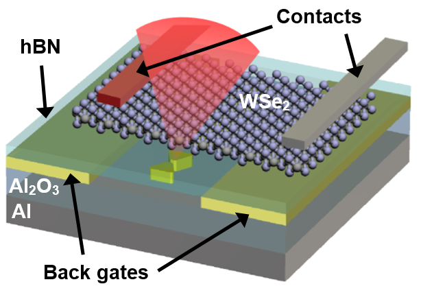
Figure 1: Device schematic showing back gates, back reflector, contacts, and light emission from a bowtie antenna.
Spontaneous emission has been considered slower and weaker than stimulated emission. As a result, light-emitting diodes (LEDs) have only been used in applications with bandwidth <1 GHz. Spontaneous emission is inefficient because the radiating dipole is much smaller than the wavelength and such short dipoles are poor radiators. By attaching an optical antenna to the radiating dipole at the nanoscale, the emission rate can be significantly increased enabling high modulation bandwidths theoretically >100 GHz. This project focuses on the physical demonstration of this new type of nanophotonic device. Current fabrication and experimental results of devices using transition metal dichalcogenides (TMDs) as an efficient nanoscale emitter material will be presented.
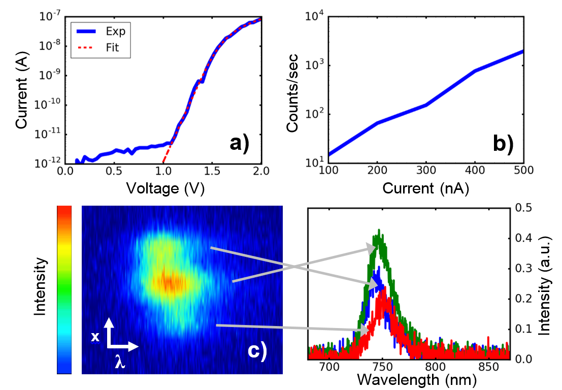
Figure 2: a) Current versus p-contact voltage, fit to diode equation with series resistance. b) L-I curve of device. c) Position vs. wavelength spectrograph of light emission, with individual peaks plotted on the right.